

It been nearly 5 years(!) since I posted my original ‘Tour of a Hoppe’s Brain GFA-555 Restoration”
A lot has changed since then. That restoration didn’t benefit from a new Hoppe’s Brain BFA-555 input board, or a binding post kit, and it uses an earlier version of my soft-start for the GFA-555. (Which is still a good power supply, but my new Smart Soft-Start BFA-555 power supply is better.)
So I’ve started taking on new refurb customers, at a much slower pace, and for a lot more money. 😸 I realized, like many small business owners, I have been under-charging for my work. The following is what you get when you drop some coin with me.

Looks pretty good. A little rash on the front panel. I’ll touch up these scratches best I can.

Pretty clean actually! Completely original, does not appear to have been worked on previously, so that’s great!


One of the shields on the RCA jack is pulling loose, a common issue. They’ll be replaced with nice Rean chassis-mount RCA jacks.

Someone has replaced the rail fuses once upon a time… one was a 3A instead of a 6A, and one was just a little melted; You can see a little blob in the middle of the wire, and it’s discolored. This fuse was red-hot at some point but didn’t quite melt.

Despite the blown fuses, this channel appears to be working perfectly. 0.018٪ @2.8V.

The amp appears to be working fine, but both channels will inspected more thoroughly before I start tearing it all down. I want to know if there are any ill conditions that might affect the condition of the output stages or power supply. I’ll check bias levels, drive currents and, as long as it’s working, I’ll check the matching of the output transistors, so if I need to replace them I can plan ahead for it.
Here’s how to check output transistor matching in-situ: The amp is connected to a dummy load, and a 1KHz, 0.125VRMS signal applied. AC Volts RMS is read across each emitter resistor to give the current through that transistor. One probe lead is attached to the positive output binding post, and then I probe each emitter.

The hottest transistor measured 41mV, and the weakest one, 31mV. Divided into 0.82 ohms emitter resistors, that’s a span of 38-50ma for each output. That may seem a wide span, but this is at only 1 Watt output, and this reading is typical. They get closer at higher currents.
The test is repeated at 1V input, 22V output, and I get a minimum of 319mV/389mA and a maximum of 324mV/395mA Less than 2%!
So it’s all good!
Teardown time!
Here’s a common issue with the original GFA-555. This LED dropping resistor for the power LED runs hot and scorches the fiberglass. The color bands are de-laminating on this one. I won’t be replacing it, the Hoppe’s Brain Smart Soft-Start power supply board runs this LED off 12VDC instead.

I put a new power switch in every amp I work on, but out of curiosity, the old power switch is disemboweled. Many of these switches arc-weld themselves shut after a while. This one is in good shape and has plenty of the ablative pad material left. High-current switches are actually designed to spark when they are engaged, forming a tiny spot-weld with low impedance.

I start tearing everything out, except the power transformer can stay where it is…

Oof! Turns out this transformer is a bit loose! I tighten it up a bit… not too much! Over-tightening a transformer can damage the windings and possibly cause a short or open.

This foot is dented in a bit, from a small drop, apparently.

Nothing a little percussive persuasion can’t fix…


Down to the metal.

New and old input boards.

The LED wires, thermal breakers, and two 16ga ground wires are installed on the new board.

The Hoppe’s Brain board has two ground wires instead of one as OEM. One is signal ground as original, and the other is ground for the local supply bypass caps, which are an additional feature of the Hoppe’s Brain boards. A separate ground wire keeps charging pulses out of the signal ground path. The signal ground goes to the top of the star-ground bolt, where it is not modulated by charging pulses. The so-called “quietest” part of the star ground.

Power supply caps are put in place, with careful attention to polarity! (Or they go boom.)

The power supply boards are centered on the capacitors as square as I can get them, and the capacitor clamps get tightened.

Power supply boards mounted

Primaries connected

EXTRA CREDIT TRANSFORMER WIRING: Normally a single wire goes from the transformer center-tap to the star-ground bolt. Capacitor charging pulses are conducted along the ground buss-bar between the capacitors. This modulates and puts noise on the star-ground. That’s not really a big problem, because the amp’s idea of “ground” is all referenced to this point, and this noise and modulation is mostly ignored by the amp… mostly… I think it’s better to move those charging currents off the star-ground, and move them directly to the capacitor grounds.
A split is made in the transformer center-tap wire, and a separate ground wire is sent to each channel’s set of filter caps.


This also tightens the loop area formed by the transformer secondaries and their ground returns. The return wire is wrapped around the supply wires., so it should radiate less EMI especially at higher harmonics caused by rectifier switching.
A Hoppe’s Brain Earth-Loop Breaker is installed, and a hole for the safety earth bolt is drilled, and paint removed around it.

Output modules next!

They need new driver transistors. The original ones are perhaps the #1 cause of GFA-555 blow-outs, though I should stress this not at all a common occurrence, and the GFA-555 is very reliable as stock. But these 2SB595/2SD525 transistors only have a VCE rating of only 100V, and the GFA-555 can swing 160V rail-to-rail! The fact they don’t intermediately blow out suggests that Adcom was testing batches of transistors for reverse breakdown, and hand-picking the high-voltage ones to go into the 555’s and the lower-voltage ones to go in the lower-voltage amps like the GFA-545 and GFA-535. This wasn’t Adcom being cheap or anything, this is more about available technology in the early 80’s. High-voltage, high current, high gain and low capacitance are all competing requirements in a driver transistor, and they didn’t have the luxury of modern devices like the On Semi MJE15032/33, which is what I’m installing… along with a C0G type compensation cap.

Bypass capacitors are added to the output modules, as in the GFA-555 II:
100uF/100V Kemet ESU in Parallel with a 0.1uF Kemet R71 Polypropylene. A bit of unused PCB trace is cut and isolated to become the ground point, and 16ga ground wires attached. These will go back to star ground.

On to the back panel! This is the last major piece before I start putting it all back together.
New RCA jacks, a Hoppe’s Brain Binding Post Adapter Kit, the Remote Trigger input, and a Neutrik Powercon Inlet.

Another extra-credit modification: As OEM, the Zobel network is located on the input board, connected by thin wires running from the output binding posts. The Zobel is an R-C network consisting of a 5.1 ohm resistor and 0.1uF capacitor in series, placed across the output of the amp. The Zobel’s purpose is to provide a short return path for high-frequency currents, from the driver board, through the base-emitter junctions of the output transistors, and returning through the negative speaker wire… Without the Zobel providing this shorter path, these currents would have to go all the way out to the speakers, through the speaker wires and back… not gonna happen, too much inductance in the speaker wire, so the Zobel provides a short path for these currents, which stabilizes the amp.
A better place for the Zobel is right across the speaker outputs, the same point that the negative feedback is taken from. (So the Zobel’s effect is included in the negative feedback.)
The 5.1 ohm resistor and 0.1uF cap are soldered directly to the binding posts, and zip-tied in place.

A single wire is run from the positive output binding post to the Feedback input. The black wires from “SPK GND” to the negative binding posts are deleted.

The back panel with the input board is installed.

Output sections get ultrasonically cleaned. This is the “dirty wash” part of the process, to wash the majority of the gunk and dust off the boards. The solvent in this bath is some very used and polluted ethanol; it’s turned orange from all the flux dissolved in it.


Then, a bath in clean ethanol to remove the flux residue from the dirty wash. The output modules don’t quite fit inside the tub of this smaller ultrasonic cleaner, so they get brushed down.

Clean! The solvent is then blown off with compressed air.

Now it’s all coming together! Output modules get installed, and their wires connected.


It works!

0.0047% THD+N :^} 0.125VRMS input, 2.77V output. No load. In reality, distortion is even lower than this, as this is about as low as my HP 8903B can resolve. As far as it can tell, this is a straight wire with gain.

The Plastic PA Horn of Truth: I use this ultra-efficient PA address horn to listen to the hum and noise of the amp. In this case there is simply nothing to hear! I can put my ear right up to this speaker and I hear dead silence. They are not this quiet from the factory, they have a faint audible buzz.

The amp is passing all the basic checks, so I am confident it’s all correct, but it will need additional testing. But first I’ll tie up all the wiring.
A thousand zip-ties later…


And the front panel.

Last step before its done!
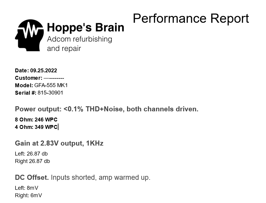
Stress tests and performance report. The amp is hooked to a dummy load, and a number of tests are run with my HP8903B Audio Analyzer, which is controlled by my laptop computer via USB-HPIB. I run a series of scripts written by Pete Millet to plot frequency response, distortion, etc. Thanks Pete! Below is just an excerpt, there are more tests run than shown here.


That’s all! This amp is ready for another 30 years or more music.
you are my hero! such good work!
Chris is nothing short of a electronic genius, with the skills of a literary, photo, artist to boot!
My hat is off to him.
Wow!