Printed circuit board+Pogo pins=Test jig.

Every circuit board I sell need to be thoroughly tested, and measurements taken that should agree with expected values. Tests are chosen to show up any errors I might have made in the board’s assembly.

- Gain. I use 0.1% tolerance resistors in key parts of the circuit, so gain should match within 0.01db from one board to another. This close gain matching is in-audible, but helps to expose potential issues with a board.
- DC operating points, such as the drive voltage to the output sections, DC offset, DC servo output, and bias voltages.
- Distortion; it should match measurements from other boards, all the way up to full-scale output.
- Current running through various branches of the circuit.
- Functionality of indicator LEDs.
Here’s how I build my test jigs.
This particular jig is designed to test my new board for the Adcom GFA-565, the EBFA-565.

- Power and ground
- BNC Input from a test oscillator
- BNC Output to oscilloscope, distortion meter, spectrum analyzer, etc.
- Indicator LEDs for clipping, thermal cutout, etc.
- A switch to loop-back the output to the input, to take a decibel reference level measurement for amplifier gain measurement.
- Miscellaneous connections; In this case, bias compensation transistors, and switches to turn bias on and off.
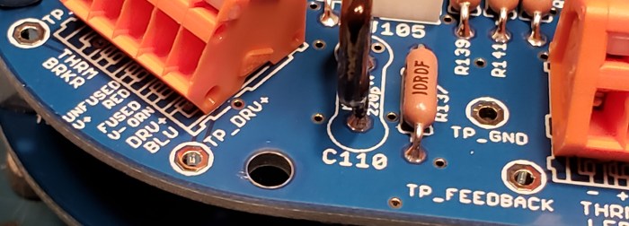
To make things even easier, the EBFA-565 board has test points for all the parameters I want to check. (Shown here as TP_GND, TP_DRV+, TP_FEEDBACK, etc.)

Connections to the underside of the board are made with these Mill-Max Pogo Pins. These pins will compress to just under 10mm, and are designed to be used with 10mm board-to-board clearance. 10mm hex standoffs are used to mount the circuit board to the jig at the correct height.

The pogo pins mate with 1mm circular test points built into the bottom of the circuit board.

Getting the pogo-pins precisely aligned:
How to get the pogo-pins to hit their target pads precisely? If you try to solder the pogo-pins in one-by-one, they will all be horribly crooked, not centered, and will miss the small 1mm test pads on the bottom of the board.
THE TRICK: Use another test-jig circuit board to hold the pins in perfect alignment while you solder the pins in place, like a pogo-pin sandwich. So, before soldering anything…
First we need to install the feet and 10mm hex standoffs. I’m fashioning the feet from an 18mm M3 hex bolts, with a nylon lock-washer. There’s lots of ways you could do this.

The 10mm hex standoffs go top-side.

Insert a pogo pin into every single spot that gets one. I put a drop of flux on each of these pads.

Take a second test jig PCB, and place it down onto the pins, and wiggle and finesse it around until the tips of all the pogo pins, snap into the holes in the second test jig board.

Now, fasten the mounting screws and your pins will all be in perfect alignment, sandwiched between the two boards.

Check that each pin is snapped into place, and if any are off, tweak them with a tweezers.

Solder from below!

Done. (Yes this happens to be different board than we started with; this is for the BFA-555 II.)

Interesting Parts:
Pogo Pins: Mill-Max 0978-0-15-20-75-14-11-0 (Suggested PCB footprint: A 1.9mm round pad with a 0.5mm drill)
Hex Standoffs, 10mm, M3 5.5mm drive: Keystone 24403
BNC Jacks: Molex 73100-0105 (Low profile to fit under 10mm pogo pins)
Test Probe Jack: Cinch Connectivity Solutions 105-0753-001
Power Jack: Molex NanoFit 105313-1303 (You’ll also need matching plug housing and pins)
Update: 2024.09.18:
Another cool jig! This one is for the Adcom GFA-555 MK1, and features a replica of the entire output section, but with just one pair of transistors and minimal heatsinking, as it will not be actually producing much power under test conditions.


I would like to say that this blog really convinced me to do it! Thanks, very good post Pogo Pins
Would love to see your results!