
~or~
How to build excellent circuit boards and install them in an amplifier
This document is meant to serve as a guide for EBFA-565 builders, as well as a general guide to building excellent circuit boards.
This is a companion document to the original GFA-565 and GFA-585 Circuit Board Replacement Notes, but does not replace that document! It is still recommended reading if you are building an EBFA-565 board.
Also highly recommend! YouTuber XRayTonyB did an excellent 3-part repair video of a GFA-585 using Hoppe’s Brain input boards. The GFA-585 is essentially identical to the GFA-565, and Tony’s video is helpful to anyone fixing a GFA-565 or GFA-585. All of his videos are entertaining, thorough and informative.
First, a word about soldering:
Flux.
Good soldering is less about solder than it is about flux! Solder flows to where the metal is clean and hot. Clean, hot solder flows like water, pulled smooth and shiny by surface tension. A smooth shiny joint has even metallurgical temper throughout.
So before I even solder one joint, every pad gets pre-coated with flux.

First, I coat the bottom of the board with old-fashioned rosin flux, diluted with alcohol. (I use ethanol, nevermind that it says isopropyl on the can.) I’m only applying it to the bottom side for now, and I’ll apply another coat to the top side after I install all the resistors and other low-lying components…

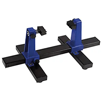
The boards is clamped into my Pan-a-vise 315 Circuit Board Holder.

The Pan-A-Vise system is a bit of an investment, and I highly recommend it, but for less than $20 you can get a circuit board holder like this one. I don’t have a specific model recommendation, but these types work good.
I start by installing the resistors and diodes, as these are low-lying components that can be soldered from the top side. Generally speaking, we place components in order of their height above the board.
Referring to the parts list, I count out exactly how many of each part I need, place them and move on to the next item. If I ever find myself holding a part with no place to go, then I know I must have misplaced something earlier on. This serves as a double-check against misplacement.

This Pace Component lead bender works fantastic! It’s fantastic plastic, not because Pace were being cheap, but because it won’t scratch or nick component leads or bodies. It’s been very durable for me.
Using this tool keeps bending strain off the component leads, and it makes them perfectly spaced so they drop right into the board.

I’m using Vishay/Dale RN55 and CMF55 for most of the resistors. Their leads are bent so their values can be read face-up.

Bottom view. Thanks to the Pan-A-Vise clamp holding the board above the bench, and working from above, I don’t need to bend the leads to keep the components in place while I solder them. This makes them easier to de-solder and remove if the board needs rework.

Almost ready to start soldering the resistors, but first, more flux is applied from the top. Now the board is coated in flux on both sides, on every pad, and in every through-hole.

Soldering the resistors from the top side: Connections on plated-through-hole circuit boards are generally more reliable than single-sided boards, because the through-hole fills up with solder and makes a firm grip on the copper plating lining the hole. Though it is not strictly necessary from a reliability standpoint, I like to have a have a “fillet” of solder on the top and bottom of each component pad. When I do a final visual inspection, I’m looking for that shiny fillet on every pad, on both sides of the board, and this serves as yet another check against missing solder joints.

Soldering Iron Temperature: A common mistake is using a too-hot soldering iron. This burns up the adhesives that hold the board together, and the copper may de-laminate. Overheating can also damage components. I recommend 660F/350C, which allows for long enough dwell time on each joint, for the heat to flow through to the other side of the board, and for the solder to wet and flow through.
My go-to solder is this Chip Quik SMDSW, water-washable, eutectic alloy. “Water-washable” means it cleans up easily and it comes off almost instantly in the ultrasonic cleaner. I don’t recommend rosin-core solders like Kester 44 for circuit board assembly. Kester 44 is great stuff—absolutely classic—but the flux is meant to be left behind, so it hardens to a waterproof, hard, amber-like substance that hermetically seals the connection. This is by design, but it makes it hard to remove.
This Chip Quik solder is decribed as “No clean” but actually… it should be cleaned, as it leaves behind a sticky residue that attracts dust. And being water-soluble, it may absorb moisture from the atmosphere.

Clipping the leads. Check that each is soldered, and if it is, it should make a *PING!* sound instead of a THUD.

Next I’ll install the SMD stabistors on the bottom of the board. The EBFA-565 board supports three types of stabistors. (A stabistor is a type of diode with an especially steep curve for current versus forward voltage, commonly used for bias stabilization in amplifiers.)
- The original KB262 and KB362. These contain two and three diodes in series, respectively. Caution: These little epoxy-blob style diodes have their anodes marked with a black stripe instead of the cathode. Verify cathode and anode with your meter on diode check. Some GFA-565’s came with glass-bodied stabistors that look just like 1N4148’s and these have their cathodes marked with a stripe per usual convention.
- Central Semiconductor CMXSTB400. These SOT26-6 packages contain four stabistors in series on one chip. The extra diodes in the package go unused. The CMXSTB400 appears to be going extinct. At the time of this writing, Mouser has less than 300 in stock, and they are “special order”.
- BAS17, which is the only type of stabistor still manufactured to my knowledge. The BAS17 is cheap as chips, but it’s only one diode per package, so you need to install 10 of them on a BFA-565 board. But they’re pretty easy.
Here’s how I do the SMD stabistors; Grab the stabistor with a tweezers. Align it perfectly square on the component pad, and use the tip of the soldering iron to push it flat to the surface of the PCB. Tack the leads to the pads with a fine-point iron. It’s not necessary to add any solder to the pad first, there is already a thin layer of solder coating the board, from the HASL (Hot-Air-Solder-Leveling) PCB manufacturing process. It will stick well enough to hold it in place.

Add more flux! Always lots of flux, I’ll be cleaning the board anyway.

…and solder each pin.

Testing the stabistors: Put your meter in diode check mode, and check the voltage drop across the stabistors. You should get about 1.2-1.5V across the KB262 positions (two diodes in series) and about 1.8-2.2V for the KB362’s (three diodes in series).

Adding a few more small components, the op-amp, trim pot, JST connectors…

Then all the capacitors and WAGO cage-clamp terminals…

Transistors next! I’ll start with the matched pairs for the input section.

Thermally bonding the input transistors:
Wrap copper foil around the transistors in the orientation they will sit in the board. Be careful the foil doesn’t touch any leads. The KSP42 and KSP92’s should be attached front-to-back as shown, and the MPSA13 and MPSA63 go face-to-face.
No thermal paste! It’s not needed, and might eventually seep oil onto the board, which attracts dust. The copper foil does a great job keeping the transistors tracking thermally, no paste needed.

Install the transistors and heat-shrink around them.

Snip the tops of the heat-shrink.

The remaining KSP42 and KSP92—for the current source section—get these heatsinks installed. No need for thermal paste, it would only make a mess. They are well cooled with these, the originals weren’t really even a problem as far as I know, but they run finger-burning hot without heatsinks.

Make sure the faces of the transistors match with the outline of the board. The KSP transistors and the original 2SC/2SA types have different pinouts, and the board supports either.

Install the rest of the transistors and the voltage references.

Last piece is the
TO-126 VAS transistors
(More specifically, these are cascodes in the VAS stage)

Apply a thin layer of thermal paste to the transistors. Use as little as possible, just enough to fill any gaps. Just enough to be opaque white. If a lot squishes out the sides when you tighten the screw, it’s too much.

Note: The heatsinks are grounded, so if you are using a metal backed transistor, such as the original 2SA1210/2SC2912, install an insulating thermal pad. The OEM heatsinks are not grounded and did not come supplied with a thermal pad.
Attach the transistors to the heatsink with the 10mm hex bolt and nylon-insert lock-washer. Use a 2mm hex driver and a 5.5mm nut driver. Apply light torque; the nylon insert lock washer will not let the bolt come loose over time.

Install. You’ll need a chonky soldering iron tip to solder the heatsink mounting pins.

Done! Now for the
Cleaning…
I like to use ethanol for cleaning PCBs, and not water-based solvents, so that if any liquid is left in any crevices, it will evaporate quickly and not cause corrosion. Use good ventilation when working with alcohol solvents. I use 200 proof Bitrix denatured ethanol, and if you google that, you’ll find it for sale online.
This is the “dirty bath”, to get the majority of the gunk off. The ultrasonic cleaner is full of well-used denatured ethanol, heated to 50C. The board gets 5 minutes ultrasonic cleaning in the dirty bath, then flipped over for another 5 minutes.


Blown out with compressed air. (Actually I do this outside.)

Now the board is mostly clean, but has a hazy film of old flux on it. So it goes for a “clean bath” in another, smaller ultrasonic cleaner, filled with fresh, clean ethanol. This unit isn’t big enough to fit the whole board, so I flip it around in the tub a few times. You can often find small ultrasonic cleaners like this at thrift stores.

The board is blown off and it’s sparkling clean!

Time to inspect everything. I’m looking for mistakes in component placement, backward diodes and transistors, metal debris, solder bridges, flux residue, missing solder joints, starved or overloaded solder joints…
Probably the most common issue my customers run into, turns out to be metal debris or solder blobs stuck between pads, or carbonized flux residue causing DC offsets and other weird issues.

Board testing time:
This is my custom test jig, or “fixture” for testing boards. It uses spring-loaded pogo-pins to make connections to the bottom of the board, with connections for power, input and output, etc… Basically, it simulates the board being installed in an amp, so that tests can be performed.

If you want to test your board before you install it in your amp, and risk blowing up your output sections… and I highly recommend you test your board, this can be done pretty easily, even without a jig. The procedure is here in the older BFA-565 installation notes document. The procedure is the same with the older version of the boards, except you won’t need to solder anything to the board, because of the WAGO cage-clamp terminals.
Board mounted to the test jig.

The signal generator is set to 1KHz 0.125VRMS, which should result in about 2.8VRMS from the board. Fingers crossed, I watch the scope and start cranking up the variac.
Success! 0.0038%THD+N at 2.8VRMS. Reality is actually even better; this is about as low as my HP8903B will measure.

Just from the distortion reading, I can tell this board is almost certainly working perfectly. But it still needs to pass a number of tests before I risk installing it into an amp. Your board came with an annotated schematic printed on 11×17 paper.

DC operating points should be checked, and you are encouraged to check each and every point noted in the schematic.
Annotated EBFA-565 schematic PDF
At minimum, check for:
1. DC voltage at positive and negative drive; DRV- and DRV+. These should be around positive and negative 1.6-1.9V, and they should be within 0.1V of each other, but opposite polarity, once the board has warmed up and the DC servo has stabilized. (Up to 2 min)
2. +/-13.8V supplies. Sagging voltage at these supplies is often due to the servo trying really hard to correct for an offset.
3. Voltage at current sources; TP_CCS+ and TP_CCS-, around +/-1.2V
4. DC offset at TP_Feedback should be less than 5mV, once the board has warmed up and the DC servo has stabilized. (Up to 2 min) May be as much as 200mV on startup. The servo takes a couple of minutes to settle, due to its very slow time constant.
5. Output of DC servo should be within -6V to +6V; TP_DCSERVO. Outside this range suggests an imbalance somewhere the servo is trying very hard to correct.
6. Clipping of the input board should occur around somewhere above 2VRMS input. Observe the output waveform on the scope and see that it clips evenly on the positive and negative halves, and that there are no visible oscillations on the clipped edges. If you have a distortion meter, you should get readings better than 0.005% with 1KHz, 0.125VRMS input, and 2.8V output. My HP8903B typically shows 0.004% in this test. However, the reality is actually better than this, as this is near the lower resolution limit of the HP8903B.
If you’re confident your board is running well, the next step is…
Installing into the amp:
TESTING YOUR OUTPUT MODULES:
FIRST! Make absolutely sure your output modules are OK. A bad output module can blow up a good input board, and troubleshooting and repairing such a scenario can become very time consuming.
It’s almost a shame to take this perfectly good BFA-565 board out! This amp is working great, but it’s going to be and Even Better F–cking amplifier by the end of this document.

The board is removed:
Incidental detail: Here you can see how I did the output connections. I’ve removed the buss-bar that ties the NPN and PNP outputs together, in favor of running a 12ga wire from each output module, to a common point on the back of the binding posts, which are tied together in parallel using 12ga solid wire. The feedback wire is attached to this point, and the zobel network, consisting of a 6.8 ohm 5W resistor in series with a 47nF Polypropylene capacitor, is connected across the 12ga solid wires, and zip-tied so it doesn’t vibrate. The body of the resistor shouldn’t touch anything, it could get hot if a fault occurs.

Remove the clip LED and thermal protection LED hookup wires from the old board. Strip approximately 4mm insulation from the ends of these wires in preparation to be inserted into the WAGO cage-clamp terminals.
Remove the thermal fuses from the old board and strip 4mm insulation from the wires.
Input board ground wire:
The only wire that needs to be permanently attached to the input board, is its ground wire, known as point 18 in the schematic. The original ground wire can be used, or make a 14ga wire that is the correct length to go back to the star-ground point on the top of the big filter capacitors, ending in a ring terminal. (Or long enough to reach the terminal block of the Hoppe’s Brain BFA-565 power supply board.)
Incidentally, if you are not installing a Hoppe’s Brain BFA-565 power supply along with your input board, The star-ground bolt should be stacked in the following order, for best noise performance. From top to bottom:
- Input Board
- Speaker ground
- Bypass cap grounds from output modules
- Big capacitors
This keeps charging current pulses away from the input board and speaker ground, while referencing these signals to each other.

Attach the mounting rails to the EBFA-565 board and install.

Hooking up the wires:
I take my time to plan ahead and wire things as neatly as possible. You’ll notice I have removed the large buss-bar that connects the outputs of the PNP and NPN modules, in favor of connecting these outputs to a common point at the binding posts. (As seen in one of the photos above.) You can use the buss-bar arrangement as OEM too, nothing wrong with it but I like this method.
Overall, I am wrapping the wires to the output modules around their power and ground wires, so that loop areas are minimized and the electric fields have some return path other than the chassis. The yellow and white wires that run between the output modules should not lay on the floor of the chassis, but they should be bundled and wrapped around the power and ground wires.
More photos of how I lay out the hookup wires.


That should be it! Double and triple-check everything is hooked up right. Don’t let the magic smoke out.
Powering up:
I’m going to bring the amp up on the variac, so I bypass the soft-start resistor. (It will burn up otherwise, because the relay will not kick in at low supply voltage.) I’ve used a jumper wire here, but you can also just move the brown wire to the COM terminal on the relay.

I apply 0.125VRMS, 1KHz to the input and slowly bring up the variac. Signal should appear when supply voltage is up to about 30%.
Success! 2.8V output, 0.004% THD+N

I ramp the variac up to 120VAC, and the amp seems to be behaving. So I unplug it from the variac and plug it straight into the outlet. Nothing smokes or goes pop, phew!
MORE tests:
Now that the amp seems to be running fine, I check all the same points as I did earlier, listed above…. Drive voltage, DC offset, etc…
Setting Bias:
Spec is 24mV across test points TP201 and TP301, which gives the voltage across two emitter resistors in series, so there is actually 12mV across each emitter resistor.

I don’t use the OEM test points. Instead, I am looking for an average of 12mV through each output emitter resistor. It’s easy to get a reading on each emitter resistor. Insert one multimeter test lead into the positive output binding post, and then probe each output transistor’s emitter, which shows the voltage across that emitter resistor.

Put the cover on the amp and let it warm up and stabilize in temperature. Check your bias levels and adjust them until they are averaging around 12mV. Rinse and repeat as necessary until you’re happy with it.
Yet more tests:
Performance tests:
Using my HP8903B Audio Analyzer,

I collect these statistics and compare them to previous amps I’ve worked on. Thanks to Pete Millet for his HP8903 Software, which allows for performance graphs to be easily plotted on a PC.
Gain: 1KHz, 0.125VRMS input: 27.19db
DC offset: <1mV
Power output: <0.1% THD+Noise, 1KHz both channels driven.
8 ohms: 324W
4 ohms; 568W
2 ohms: 928W
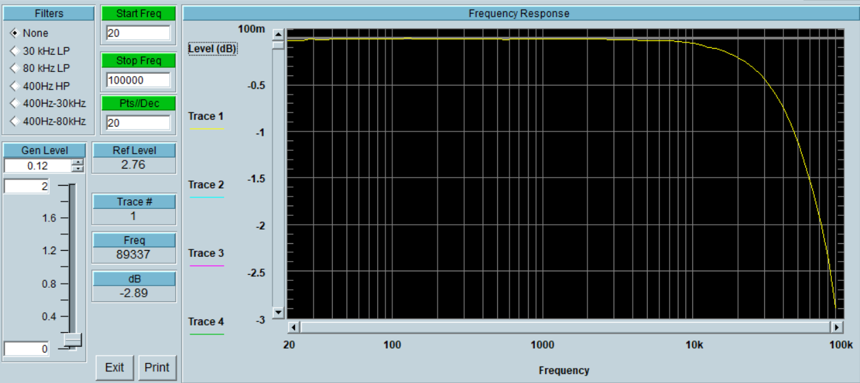
Frequency Response: 1KHz, 0.125VRMS input, 2.8VRMS output
Power vs THD+Noise, 8 ohm, 1KHz

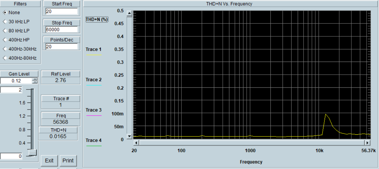
THD+N v frequency 4 ohms, 0.12V input 2.8V output, 20Hz- 60KHz
Spike at 13KHz is something in my system, not sure what, but it shows up in all my measurements.
Square-wave open-circuit:

Square-wave into difficult load: 1uF in series with 2 ohm. 20Vp-p, 50uS/div

Looks great! It is…
DONE!
Enjoy the music.